I was thinking about prototyping electronics again, as I often do, and I was wondering about what might be optimal (as in most flexible) for handling small SMT parts like SOT23-3.
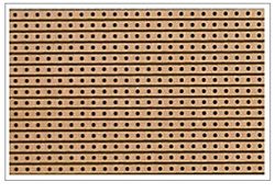
Your choices are many, but pretty much all are bog-standard offerings derived from the original Veroboard layout (i.e. 0.1″ hole array, with a series of parallel traces on one side) or just an array of holes.
The rights to ‘Vero Board’ have been passed around a fair bit, but they are now settled with a UK company, Vero Technologies. Conveniently, they are very close to where I live, so one day, I may visit them.
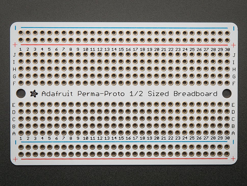
Various people have tried to make better prototyping boards over the years. A good example is the Adafruit Perma-proto, which is designed with an emphasis on quality since Limor was fed up with the poor quality protoboards available. You can get these directly from Adafruit’s main site, from one of their distributors, or on eBay.
Another, different approach that I admire a lot is to bring common hard-to-prototype footprints onto a PCB and create a sort of mixed-footprint and generic layout with a standardised format. MikesElectricStuff created a great example of this that he calls simply a Universal Prototyping Board.

I may produce something similar in the future, with my favourite footprints, but for now, you can order these directly from Mike at his website link above.
Tessellations
Anyway, none of this is what I want to talk about. Like I said earlier, I was thinking about SOT23-3, which is a three-pin footprint. Asking questions like “What’s the ideal environment around such a thing?” “What if it’s a MOSFET?” “How about a linear regulator?” After delving into a mathematically oriented connectivity analysis, I had a simple thought – why are circuits often rectilinear? What other geometric constructs might be useful?
How about tessellations?
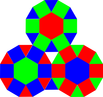
There are lots of ways for tiles to fit together. Some of the most basic shapes, such as squares, triangles, and hexagons, tessellate trivially. Let’s look at a few and review them regarding electrical connectivity.
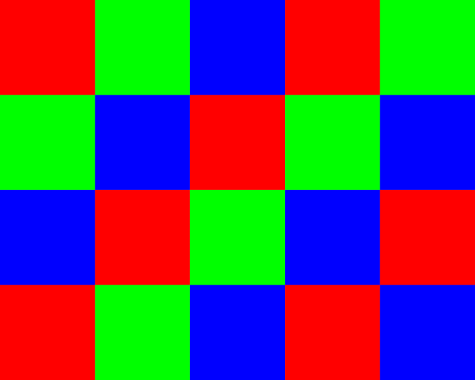
Triangles and Squares
If we consider each node in a circuit as a single tile in a tessellated pattern, then the boundary or join between each pair of tiles can host a single two-terminal device (or multiple in parallel). For example, in the triangular pattern, each node can have three devices attached, since each triangle has three edges and three neighbours.

Similarly, squares and hexagons tessellate trivially:
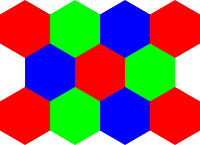
I thought about it for a while and played with some simple circuit topologies, I concluded that hexagonal-based tessellation would be most fun, so proceeded to try a few common circuits and see how easily they mapped.
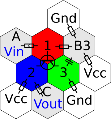
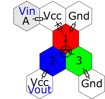
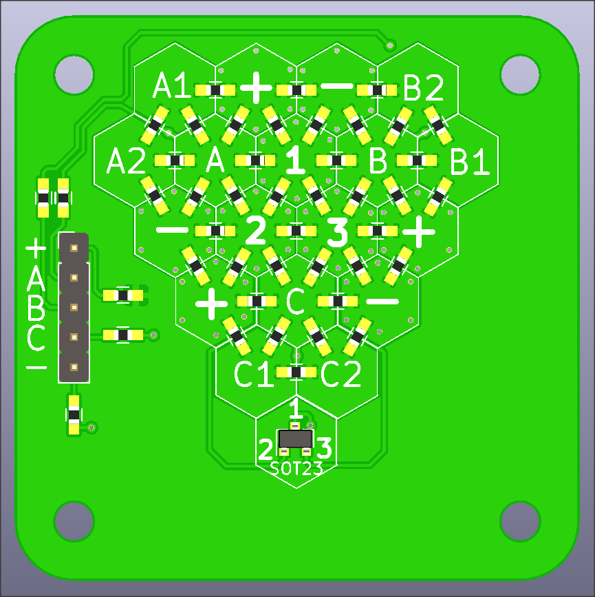
Example Hexagonal Topology
For fun, I decided to restrict the circuit to being purely defined by the component placement, so only the bill of materials is relevant. The assignment below is rotationally symmetric, so the functional pin mapping of the SOT23-3 device is not relevant.
The Red (1), Green (3), and Blue (2) tiles are the SOT23-connected nodes, corresponding to pads 1-3 of the footprint in the PCB shown later on. The lettered nodes {A, B, C} (hereafter referred to as connection nodes) and also Vcc and Gnd are connected to a pin header for interfacing with the outside world.
The White tiles are fixed-function rails intended for power and ground, but they can be any signal, really, an example of which we’ll see later.
All the above tiles have the same connectivity on the top and bottom surfaces. Grey tiles are a little different in that they have one signal mapped on the top of the tile and a different signal on the bottom.
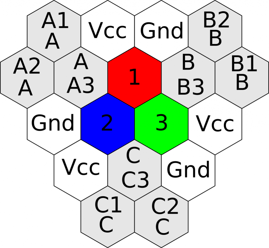
Nodes A{1-3}, B{1-3}, and C{1-3} are uncommitted or intermediate nodes and are not connected to anything else.
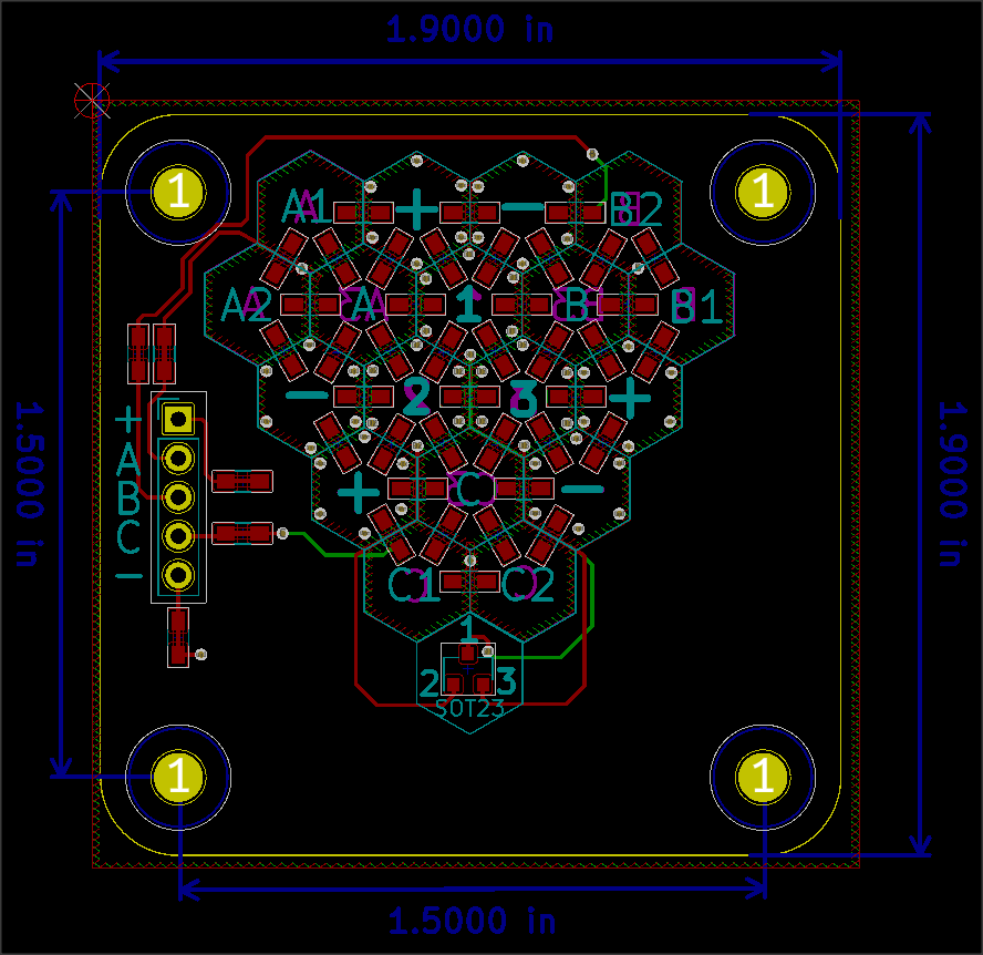
For the PCB I designed, each shared edge of every tile can take a single 0603 SMT device, with one footprint on the top surface, connecting adjacent tiles and a second footprint on the bottom surface acting similarly. The aim is to construct the circuit around the SOT23-3 device by building connections from the external connection nodes {A, B, C} using common prototyping parts such as chip resistors, ceramic capacitors, and diodes. Inductors of small value also exist in this format, as do many other less-common two-terminal devices.
Zero-ohm links can be used as jumpers to connect nodes when no other device is desired.
Trying a few circuits for size
It’s pretty simple to map a circuit onto this fixed-interconnect, just by assigning connection nodes {A, B, C} that are near to the appropriate device pin, then fitting intermediate nodes as required. Since each node can take twelve component connections, that should be plenty! Obviously, uncommitted nodes only have half as many connections, but that’s still six and should be sufficient, also.
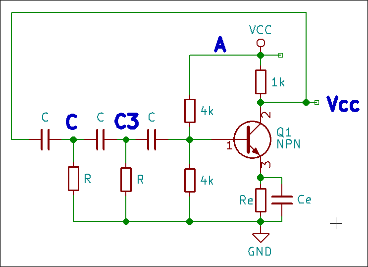
Emitter Follower
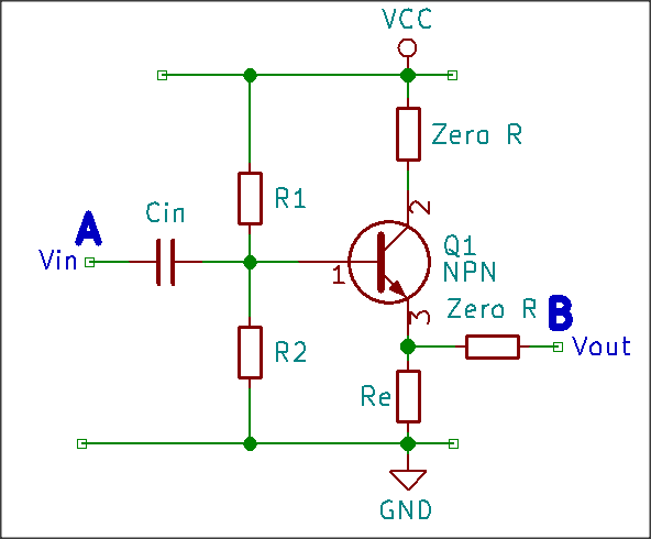
Note use of 0R links to connect device nodes {1,2,3} to connection nodes {A,B,C}

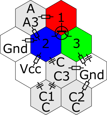
Bootstrap Bias
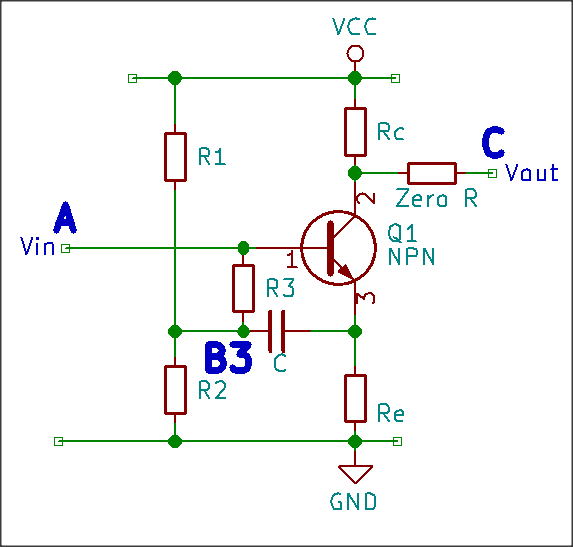
Note the use of uncommitted node B3 with parts placed on the underside of the layout
BJT Shunt Regulator
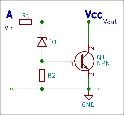
The VCC node is used as an output node.
Phase Shift Oscillator
Connection node A is assigned to Vcc, and the Vcc node is assigned to the output signal. This may not be the best naming scheme.
Example implementation
The next stage was obviously to make it real by laying out a simple PCB. The PCB is intended to fit onto my standard prototyping plastic pin board, which has an array of holes on a 0.5″ pitch.
More information
The KiCAD project files and Gerber files for manufacture can be downloaded from the CrazyProto GitHub repository. The files will be located in the HEX-SOT23 project folder. If there is any interest, I may order some in the near future.
Update 02 April 2019
After spotting a deal[1] getting super cheap PCBs from JLCPCB, I ordered a bunch, and here they are in all their HASL-finished glory. Now to find some time to build a circuit on them 🙂
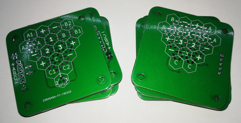
[1] Discount PCB with HASL for just $2 with Free DHL shipping China->UK. The Total Cost for 10 units is $2, or two cheeseburgers in McDonald’s currency.