Many timing-type instruments, such as frequency counters, AWGs, and oscilloscopes, can be tied to an external frequency reference, most commonly 10 MHz. This enables the correlation of measurements from different instruments and vastly improves their accuracy and repeatability.
Impedance and Termination
It is useful to mention impedance at this point. Many single-ended clocked signals are intended to be driven into a 50 Ω load. This means the driving device will have an output impedance of 50 Ω, will need to be connected to a cable with a characteristic impedance of 50 Ω, and the signal must terminate at the receiver with an input impedance of, you guessed it, 50 Ω.
Reflections
Signal reflections can occur if you fail to maintain this impedance along the signal path, provided the cable run is long enough. This, of course, depends on the rise or fall time of the signal, which is closely related to the frequency. Generally, the higher the frequency of a signal, the shorter the rise/fall time, and the shorter the cable can be before reflections happen.
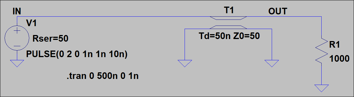
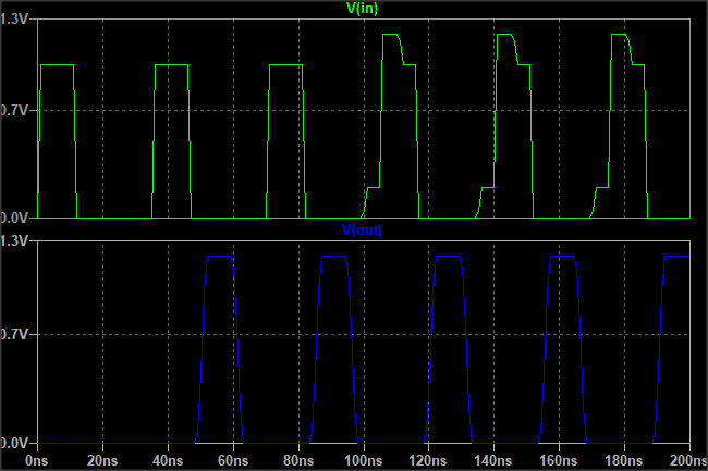
Above is a simple lossless transmission line model driven from a 50 Ω source. The driver level is set to 2v, which results in the desired signal level of 1v along the line. The output impedance of the driver and the transmission line characteristic impedance form a resistor divider by a factor of two, hence the reduced signal level. As will be seen, since the load is NOT 50 Ω, but 1 kΩ (like the reference input impedance of an Agilent 53132A), the pulse will be reflected with significant amplitude.
As an example, the Agilent 53132A timer/counter in front of me has a reference input specification of 200mV – 10v 1kΩ, so it will require an external terminating BNC 50Ω resistor connected via a ‘Y’ adaptor. However, you would have to exceed 10v before damage occurs, which would be pretty unlikely in practice.
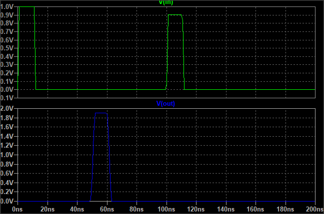
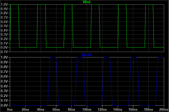
Tweaking the simulation to increase the pulse count and density, we can see how the waveform gets mangled by returning reflected pulses.
What you would actually see would be affected by the cable length, the degree of impedance mismatch, and the cable loss. I could have simulated this with a model of the RG58 Coax cable that is commonly available, but that would not have helped illustrate these points so clearly.
Perhaps I will post about that another time?

Poor termination or cable matching can really ruin your day. Best to terminate properly and not worry about it.
Signal Level
Secondly, the signal level will be wrong without the correct load impedance. This can cause the receiving device to be under-driven and fail to see the signal. Worse, if it is badly overdriven, damage can occur if the receiver is not adequately protected.
Timing Source
My lab has a GPS receiver that disciplines an internal TCXO reference to maintain a very accurate and stable frequency. This device provides 10 MHz, 1 Hz (aka 1 PPS) outputs and generates NMEA-0183 sentences over a serial port. It is very useful if you care about timing accuracy.
I need (well, I want) a rack-mount solution to buffer this 10 MHz reference clock from my GPS receiver to various instruments that take an external reference input.
Being a hacker and a cheapskate, I find commercial offerings prohibitively expensive. Offerings on Aliexpress, like this one, leave me cold.
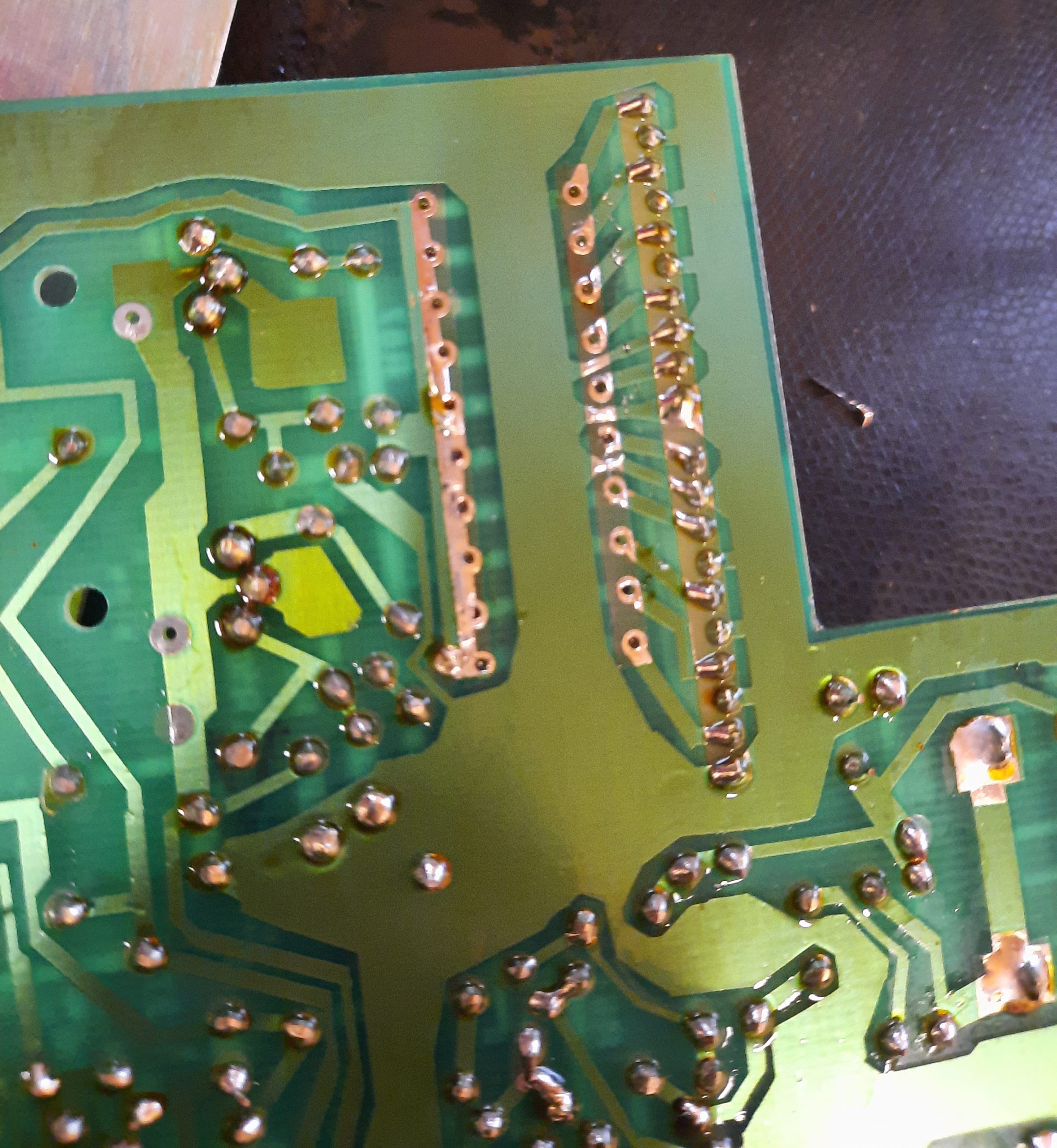
I recently read about someone modifying a video distribution amplifier (VDA) on some random forum. The idea was to swap out the 75 Ω terminating resistors for 50 Ω. These VDAs are similar to timing distributors; they take in one video signal, amplify it, and drive it out onto multiple connectors.
Anyway, I bought a used one from eBay and looked inside.
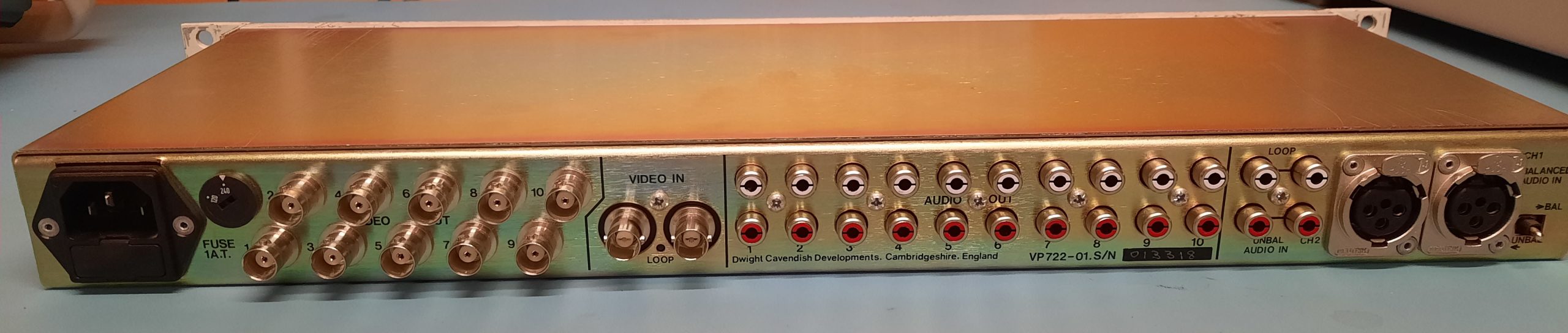
I was only interested in the video section on the left, so I ripped it open and investigated further.
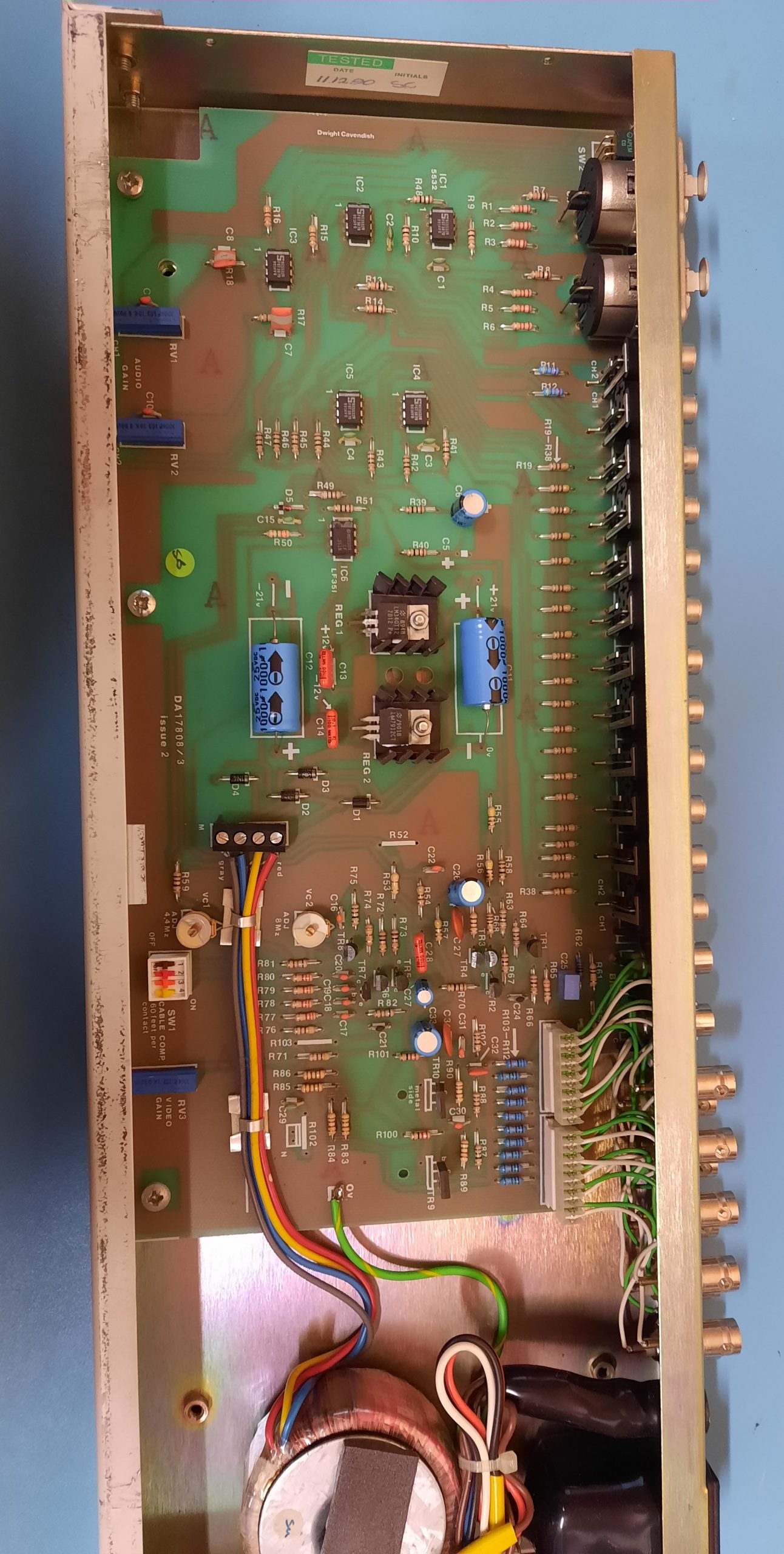
I just dived straight in and ripped it apart to remove that block of ten blue resistors at the bottom.
The Issues
Then the penny dropped. This is a single amplifier driving all outputs in parallel. That strip of copper on the left is the common side, and each output is purely connected via its own 75 Ω resistor.
This isn’t what I had in mind, and it’s inadequate for even my simple needs.
The biggest issue with this arrangement is that there is no isolation between outputs, so any noise or reflections on one output channel will propagate to all other outputs.
Output Level
The other issue that comes to mind is that the signal level would be affected. As more of the outputs are populated and terminated, all those 50 Ω loads will further lower the signal level.
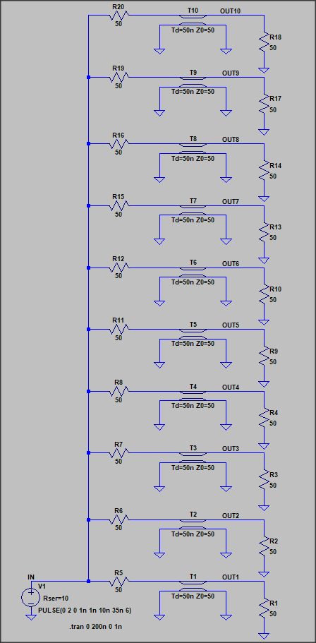
If I were to use the VDA as it is and swap out the 75 Ω resistors for 50 Ω, I would end up with a situation similar to the above: ten loads of 50 Ω being driven by a single source. I chose to model the shared driver with a 10 Ω output impedance. I didn’t measure the VP722, but it doesn’t seem too far off.
If we back off a little, disconnect nine cables and just imagine the bottom of the circuit above, with a single transmission line (T1) for now.
First, calculate Vin :
\[ V_{in} = 2 \times \frac{R_5 + R_1}{R_{V_1} + R_1 + R_5} = 2 \times \frac{50 + 50}{50 + 50 + 10} = 1.82 \, V \]
The voltage level at R1 would then be:
\[V_{R_1} = V_{in} \times \frac{R_1}{R_1 + R_5} = 1.82 \times \frac{50}{50 + 50} = 0.91 \, \text{V}\]
So, the voltage level is close to the desired 1v and could be improved with a better driver.
Now, connect the other nine loads, and the signal level would be a fair bit less; you can calculate this easily, as the effective load on the driver would be the parallel combination of all ten coax cable characteristic impedances combined with the load, or (50+50)/10 = 10 Ω
Now, that 2v pulse at the driver output, Vin would be:
\[V_{in} = 2 \times \frac{10}{R_{V_1} + 10} = 2 \times \frac{10}{10 + 10} = 1 \, \text{V}\]
\[V_{R_1} = V_{in} \times \frac{R_1}{R_1 + R_5} = 1 \times \frac{50}{50 + 50} = 0.5 \, \text{V}\]
These values can be seen in the simulation results:

To alleviate these concerns, I want a proper driver per channel. I don’t have any choice but to ditch the PCB and make something specific.
The Plan
I can reuse the case, the nice little toroid transformer. Using a linear power supply makes sense to keep the power noise to a minimum. Switched-mode supplies can add a lot of unhelpful noise if inappropriately applied to a circuit. The metal case will provide helpful shielding to keep external noise out of the box, which will help keep external noise away from the timing outputs.
Signals
In reality, we’re not really dealing with square wave signals at all in this application. I merely took a diversion to talk about this simplistically. We are dealing with a more pure signal with frequency standards – a sine wave.
The square wave would have odd-harmonic frequency components, all adding to the noise we don’t want. A sine wave has a single tone, the fundamental, and we care only about its phase and frequency.
We don’t even care about the phase so much. Correctly speaking, we’re not dealing with a problem of synchronisation (bringing systems into phase alignment) but syntonisation, which means bringing systems into frequency alignment.
I shall write about phase another day.
The distribution amplifier we desire is just that—an amplifier, not a digital buffer. We must take in a signal and drive it out with isolated outputs at a decent signal level. It can be attenuated appropriately if this level is too high for a specific device. Of course, we still need proper termination.
For instruments that use this reference signal in a digital manner, they would include input signal conditioning, typically a Schmitt trigger,
Isolation
The next matter is isolating the DC paths. A naïve approach would be to connect the shield/ground of the output BNC jack straight to the analog ground for all outputs and hook the signals straight to the amplifier outputs with a terminating resistor.
This is not necessarily bad and will work. But, it is not a great thing to do.
There are many reasons for this, including removing ground loops, isolating power supply noise paths, and addressing DC levels.
Basic electrical safety is also a significant consideration. If a power supply fails weirdly and shorts the line AC to ground in a box somewhere, you don’t want it propagated to every instrument via that common ground connection!
To achieve this, we will specify a requirement for an isolating transformer for each output. This way, there will be no galvanic connection from the outside world into the box.
Requirements
Simply put, I want:
- 10 off outputs 10 MHz sine wave at minimum 1Vrms into 50 Ω
- 5 off outputs of 1pps as above (TBD)
- Isolation for all outputs via transformers
- Linear power supply for low-phase noise
- Shielded metal case
Next Steps
The next step is to measure the PCB mounting locations and connector positions, draw up a board outline, and get cracking.
LTspice Source Code: TransmissionLine multipleTransmissionLines